Note: We have a new contributor, Konpal Ali - an enthusiastic Electrical Engineering (EE) major who tells us, in a non-dense fashion, about the nature of her recent EE project.
Making our very first EE project was pretty exciting (just the first one though, I must add). There were all sorts of ideas: a tracking device (sort of like GPRS but simpler), a model green city lit up by LED’s and whatnot. After discussing all the ideas with our Professor, it was a little disappointing to know that we were biting on much more than we could chew since this was our very first project. My project partners and I decided eventually to settle for an ultimate spy device of some sort (yes some sort and ultimate, that’s me): the FM phone transmitter.
We were happy doing this project because it had room for making the device more complex (or, in other words, for shashkay). The basic idea was to tap signals from a phone line, frequency modulate them, and transmit them in the radio frequency range. These modulated waves were then picked up by a remote radio receiver within a 200 feet range (or a much larger one if we added a tiny antenna. Another shashka), and voila - you would be able to hear what the annoying old lady next door has to say about your guitar abilities to her grandchildren. Simple as it sounds, it turned out to be pretty messy and that was when I realized how complex practical circuits can get when you are dealing with high frequencies - high frequency is not friendly.
We were to make use of the fact that in the telephone line the many frequency signals could be grouped into 3 sets:
I. The very high frequency noise we were to get rid of,
II. The low frequency signals which power the phone lines (which is why telephones work even when WAPDA decides to test our patience), and
III. The moderate frequency audio signals we wanted to spy on.
After this classification it becomes a matter of separating out the three, and simply frequency modulating the audio signals (III) required for transmission (nothing simple about that I must add).
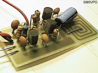
RECTIFICATION: From the phone line, our circuit (see Fig) took in a mixture of the three signals - the happy family mentioned above and first of all rectified them (conversion from A.C to D.C, for dummies). This was required because the circuit consisted of two transistors (T1 and T2), which are powered by direct current only. After this initial rectification the fun began. Resistors R1 and R2 were used as potential dividers.
SEPARATION OF SIGNALS: R1 took the happy family (a mixture of the three signals) on to the path of gloom and sorrow - separating them out. The happy family encountered what was on ‘overall low pass filter’ (see Fig), which meant the members of the happy family with high frequencies would be grounded (read: killed). Inside the ‘overall low pass filter’, the very high frequency noise (I) was grounded (killed) right away by a low capacitance capacitor C3. The low frequency power signal (II) passed through one of the branches, while the moderate frequency audio signal (III) through another branch (see Fig).
AMPLIFICATION: The power (II) and the audio (III) signals (which hadn’t been killed), then moved on to the transistor T1. T1 was turned ON by the power signal (II), and in turn did its job: amplifying the audio signal (III).
FREQUENCY MODULATION: The now amplified audio signal (III) then moved on to the LC oscillator and from here was frequency modulated into carrier waves in the Radio Frequency region so that it could be transmitted further along in the circuit. The audio signal had now officially been converted to radio waves that had the audio message we required (the new III).
AMPLIFICATION (AGAIN) AND TRANSMISSION: As the Radio Frequency is a high frequency in the spectrum, the low capacitance capacitor C7 was used to transmit the radio waves to transistor T2. By this time we did not have low frequency power signals (II) left to turn on the transistor (as they had been used up by transistor T1), which is why we had the potential divider consisting of R1 and R2 in the beginning. Some of the rectified ‘happy family’ had come down to the rescue via the potential dividers second branch (i.e. the branch containing R2), and its low frequency power signal component (i.e. II) was used to power T2 and thus amplify our radio waves. At this point in the circuit (i.e. right after amplification by T2), the radio waves were transmitted (an antenna can be placed here if a larger range for eavesdropping is required).
ACTUAL SPYING: The transmitted radio waves were tapped using a radio which had been set to the frequency of the modulated radio waves (III), and the eavesdropping process thus begun!
For people confused about Fig: C6, L1 and L2 make sure the rest of the signals from the potential divider branch coming from R2 are grounded (killed) and don’t mix with the output of the initial rectifier.
Unfortunately for my project partners and I, the exact capacitors we required weren’t available and so we weren’t able to transmit in the Radio Frequency range but in the Short Wave region and so we couldn’t use our spy device with a radio. Regardless, the whole project was a pretty eye-opening experience. There is a vast field out there, and it is fascinating how we can come up with so many applications by just messing around with a bunch of basic things. Furthermore, the biggest realization that came with this project was the fact that although Engineering might not directly involve discovery, the importance of application has always had priority. The bottom line is we discover to invent.
Konpal
Making our very first EE project was pretty exciting (just the first one though, I must add). There were all sorts of ideas: a tracking device (sort of like GPRS but simpler), a model green city lit up by LED’s and whatnot. After discussing all the ideas with our Professor, it was a little disappointing to know that we were biting on much more than we could chew since this was our very first project. My project partners and I decided eventually to settle for an ultimate spy device of some sort (yes some sort and ultimate, that’s me): the FM phone transmitter.
We were happy doing this project because it had room for making the device more complex (or, in other words, for shashkay). The basic idea was to tap signals from a phone line, frequency modulate them, and transmit them in the radio frequency range. These modulated waves were then picked up by a remote radio receiver within a 200 feet range (or a much larger one if we added a tiny antenna. Another shashka), and voila - you would be able to hear what the annoying old lady next door has to say about your guitar abilities to her grandchildren. Simple as it sounds, it turned out to be pretty messy and that was when I realized how complex practical circuits can get when you are dealing with high frequencies - high frequency is not friendly.
We were to make use of the fact that in the telephone line the many frequency signals could be grouped into 3 sets:
I. The very high frequency noise we were to get rid of,
II. The low frequency signals which power the phone lines (which is why telephones work even when WAPDA decides to test our patience), and
III. The moderate frequency audio signals we wanted to spy on.
After this classification it becomes a matter of separating out the three, and simply frequency modulating the audio signals (III) required for transmission (nothing simple about that I must add).
RECTIFICATION: From the phone line, our circuit (see Fig) took in a mixture of the three signals - the happy family mentioned above and first of all rectified them (conversion from A.C to D.C, for dummies). This was required because the circuit consisted of two transistors (T1 and T2), which are powered by direct current only. After this initial rectification the fun began. Resistors R1 and R2 were used as potential dividers.
SEPARATION OF SIGNALS: R1 took the happy family (a mixture of the three signals) on to the path of gloom and sorrow - separating them out. The happy family encountered what was on ‘overall low pass filter’ (see Fig), which meant the members of the happy family with high frequencies would be grounded (read: killed). Inside the ‘overall low pass filter’, the very high frequency noise (I) was grounded (killed) right away by a low capacitance capacitor C3. The low frequency power signal (II) passed through one of the branches, while the moderate frequency audio signal (III) through another branch (see Fig).
AMPLIFICATION: The power (II) and the audio (III) signals (which hadn’t been killed), then moved on to the transistor T1. T1 was turned ON by the power signal (II), and in turn did its job: amplifying the audio signal (III).
FREQUENCY MODULATION: The now amplified audio signal (III) then moved on to the LC oscillator and from here was frequency modulated into carrier waves in the Radio Frequency region so that it could be transmitted further along in the circuit. The audio signal had now officially been converted to radio waves that had the audio message we required (the new III).
AMPLIFICATION (AGAIN) AND TRANSMISSION: As the Radio Frequency is a high frequency in the spectrum, the low capacitance capacitor C7 was used to transmit the radio waves to transistor T2. By this time we did not have low frequency power signals (II) left to turn on the transistor (as they had been used up by transistor T1), which is why we had the potential divider consisting of R1 and R2 in the beginning. Some of the rectified ‘happy family’ had come down to the rescue via the potential dividers second branch (i.e. the branch containing R2), and its low frequency power signal component (i.e. II) was used to power T2 and thus amplify our radio waves. At this point in the circuit (i.e. right after amplification by T2), the radio waves were transmitted (an antenna can be placed here if a larger range for eavesdropping is required).
ACTUAL SPYING: The transmitted radio waves were tapped using a radio which had been set to the frequency of the modulated radio waves (III), and the eavesdropping process thus begun!
For people confused about Fig: C6, L1 and L2 make sure the rest of the signals from the potential divider branch coming from R2 are grounded (killed) and don’t mix with the output of the initial rectifier.
Unfortunately for my project partners and I, the exact capacitors we required weren’t available and so we weren’t able to transmit in the Radio Frequency range but in the Short Wave region and so we couldn’t use our spy device with a radio. Regardless, the whole project was a pretty eye-opening experience. There is a vast field out there, and it is fascinating how we can come up with so many applications by just messing around with a bunch of basic things. Furthermore, the biggest realization that came with this project was the fact that although Engineering might not directly involve discovery, the importance of application has always had priority. The bottom line is we discover to invent.
Konpal
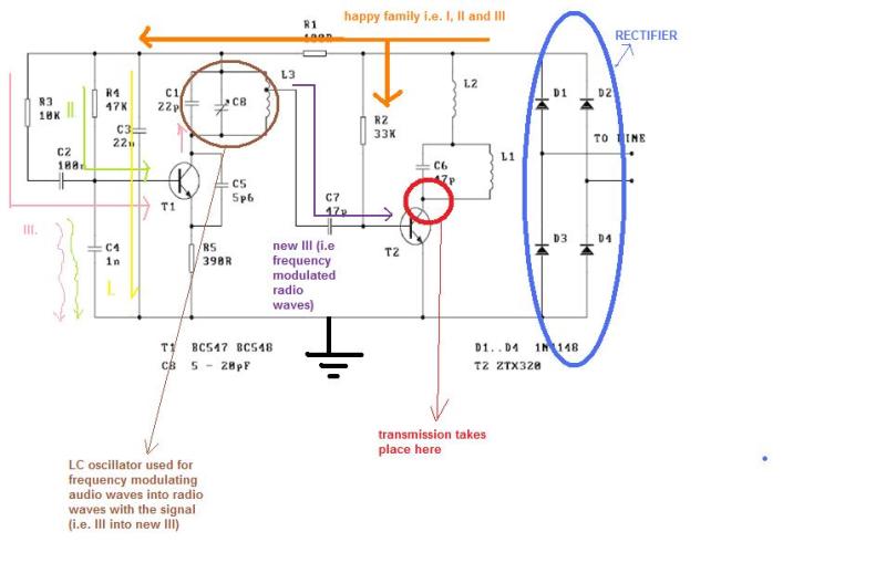
Fig.
FM Wireless Microphone Transmitter Circuit
FM Shoes


 RSS Feed